Instruction Set and their types, Functions with examples and Addressing Models of 8085 Microprocessor
Instruction Set of 8085 Microprocessor
An instruction is a command given to the computer to perform a specified operation on the given data. In 8085 microprocessor, the instructions are classified into five (5) groups. They are,
- Data Transfer Group
- Arithmetic Group
- Logical Group
- Branch Control Group
- I/O and Machine Control Group
Addressing Models:
Each instruction requires certain data on which it has to operate. In Intel 8085 Microprocessor, there are 4 types of addressing mode.
More on Addressing Models>>>
- Data Transfer Group
- MOV r1, r2
- This means the data of register - 2 will move to register - 1
Example - MOV A, B
- MOV r, M
- This means the data stored in ((H - L)) will move to the specified register.
Example - MOV B, M
- MOV M, r
- This means the data in the specified register will move to ((H-L)).
Example - MOV M, B
- MVI r, data
- This means the given data will move to the specified register immediately.
Example - MVI B, 05
- MVI M, data
- This means the given data will move to ((H-L)) pair register immediately.
Example - MVI M, 05
2. Arithmetic Group
- ADD r
- The data in Accumulator and entered register will get added and the result will copy to Accumulator
(A) + (B) ⇢ (A)
- ADD M
- The data in Accumulator and data in the memory location pointed by HL pair will get added and the result will copy to Accumulator.
(A) + ((H-L)) ⇢ (A)
- ADC M
- The data in Accumulator, data in the memory location pointed by HL pair and value of Carry Bit will get added and the result will copy to Accumulator.
(A) + ((H-L)) + (CS) ⇢ (A)
- ADC r
- The data in Accumulator, data in entered register and value of Carry Bit will get added and the result will copy to Accumulator.
(A) + (B) + (CS) ⇢ (A)
- ACI data
- The data in Accumulator, entered data and value of carry bit will get added and the result will copy to Accumulator.
(A) + (06) + (CS) ⇢ (A)
More Instructions On Arithmetic Group >>>
3. Logical Group
- ANA r
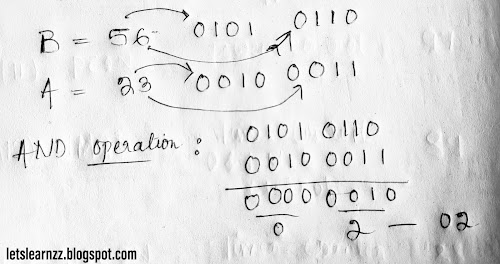
- Here the data of r AND (Logical AND) with the data of Accumulator and the result will store in Accumulator.
(B) ⋀ (A) ⟶ (A)
Data in Accumulator is 23 and data in register B is 56.
After executing the program,
Data in Accumulator will be 02
(Can't Understand Refer This Image )
- ANA M
- Here the data in the memory location pointed by HL pair AND (Logical AND) with data in Accumulator and the result will store in Accumulator.
((H-L)) ⋀ (A) ⟶ (A)
Data in Accumulator is 23 and data in ((H-L)) is 56
After executing the program,
Data in Accumulator will be 02.
- Unconditional Jump
- JMP addr
- Here the program sequence jumps to the mentioned address to the execution of next instructions.
- JZ addr
- This means the jump event will happen when Z = 1. The program execution will jump to a mentioned addr and executed that program first and then return to main program.
- JNZ addr
- Here the jump event will happen when Z = 0.
- JC addr
- Here the jump event will happen when CS = 1.
- JNC addr
- Here the jump event will happen when CS = 0.
- JP addr
- Here the jump event will happen when S = 0
- JM addr
- Here the jump event will happen when S = 1
- JPE addr
- Here the jump event will happen when P = 1
- JPO addr
- Here the jump event will happen when P = 0.
Detail Understanding Is here>>>
5. Stack, I/O and Machine Control Group
- NOP (No Operation)
- Here No Operation is performed after execution of the command. No Status Flags are affected during the execution of NOP. The instruction is used to fill in time delay or to delete and insert instructions while troubleshooting.
- HLT
- At this instruction, the microprocessor finishes the execution program. The data in registers are unaffected during Halt State.
- DI
- Disable Interrupt is used to disable the interruption during the execution of instructions.
- EI (Enable Interrupt)
- After a system reset or the acknowledgement of an interrupt, the Interrupt Enable the flip-flop is reset, thus disabling the interrupts
- SIM (Set Interrupt Mask)
- RIM (Reset Interrupt Mask)
More on Stack, I/O and Machine Control Group>>>


Comments
Post a Comment