Logical Group Instruction Set of 8085 Microprocessor | ANA, ANI, ORA, ORI, XRA, XRI, CMA, CMC, STC, CMP, RLC, RAL, RRC, RAR instruction examples

Logical Group


These Logical group instructions are used in the 8085 Microprocessor program. In this article, you would get the instructions with example. In some sections, referring images are also provided to make your understanding crystal clear.
    • ANA r
      • Here the data of r AND (Logical AND) with the data of Accumulator and the result will store in Accumulator.
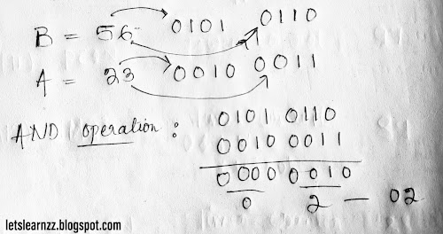
                                Example -  ANA B 
                                                    (B) ⋀ (A) ⟶ (A)
                                               Data in Accumulator is 23 and data in register B is 56.
                                                After executing the program,
                                                Data in Accumulator will be 02

(Can't Understand Refer This Image )
Instruction Set of 8085 Microprocessor


    • ANA M
      • Here the data in the memory location pointed by HL pair AND (Logical AND) with data in Accumulator and the result will store in Accumulator.
                                Example -  ANA M
                                                   ((H-L)) ⋀ (A) ⟶ (A)
                                                    Data in Accumulator is 23 and data in ((H-L)) is 56
                                                    After executing the program, 
                                                    Data in Accumulator will be 02.
    • ANI data
      • Here the data AND with the value of Accumulator and the result will store in Accumulator.
                                Example - ANI 56
                                                   (56) ⋀ (A) ⟶ (A)
                                                   Data in Accumulator is 23
                                                   After executing the program,
                                                   Data in Accumulator will be 02.
    • ORA r
      • Here the data in entered register OR with the value of Accumulator and the result will store in Accumulator.
                                Example -  ORA B
                                                    (B) ⋁ (A) ⟶ (A)
                                                    Data in register 'B' is 56
                                                    Data in Accumulator is 23 
                                                    After Execution of Program,
                                                    Data in Accumulator will be 77
(Can't understand refer this image)

    • ORA M
      • Here the data in the memory location pointed by HL pair OR with the value of Accumulator and the result will store in Accumulator.
                                Example - ORA M
                                                  ((H-L)) ⋁ (A) ⟶ (A)
                                                  Data in ((H-L)) is 56 
                                                  Data in Accumulator is 23
                                                  After execution of the program,
                                                   Data in Accumulator will be 77.
    • ORI data
      • Here the entered data OR with the data of Accumulator and the result will store in Accumulator.
                                Example - ORI 05    
                                                   (05) ⋁ (A) ⟶ (A) 
                                                    Data entered is 05
                                                    Data in Accumulator is 45
                                                    After execution of the program,
                                                    Data in Accumulator will be 45.
    • XRA r
      • Here the data in entered register X-OR with the data in Accumulator and the result will store in Accumulator.
                                Example - XRA B
                                                  (B) ∀  (A) ⟶ (A)
    • XRA M
      • Here the data in the memory location pointed by HL pair X-OR with the data in the accumulator and the result will store in the accumulator.
                                Example - XRA M
                                                   ((H-L)) ∀  (A) ⟶ (A)
    • XRI data
      • Here the entered data X-OR with the data in Accumulator and the result will store in the accumulator.
                                Example - XRI 05
                                                  (05) ∀  (A) ⟶ (A)
    • CMA 
      • This instruction means to complement the data in the accumulator.
                                Example - CMA
                                                   Data in Accumulator is 56 (0101 0110)
                                                   After Execution of the program,
                                                    Data in the accumulator will be 1010 1001 (A9)
    • CMC 
      • This instruction is used to complement the content in carry.
    • STC
      • This instruction is used to set the value of carry.
    • CMP r 
      • Here a comparison action will happen between the content of register and accumulator. Flag bit changes.
    • CMP M
      • Here a comparison action will happen between the content of memory location pointed by HL pair and the content of accumulator.
    • CPI data
      • Here a comparison action will happen between the mentioned data and the contents of the accumulator. The Sign flag will get affected.
    • RLC 
      • Means: Rotate Accumulator Left.
      • Here the content of An ⇢ An+1, A7 ⇢A0 and A7 ⇢ CS
    • RAL 
      • Means: Rotate Accumulator through Carry
      • Here the content of An ⇢ An+1, A7 ⇢ CS and CS ⇢ A0 
    • RRC
      • Means: Rotate Accumulator Right
      • Here the content of A0 ⇢ A7, A0 ⇢ CS  and An+1 ⇢ An
    • RAR
      • Means: Rotate Accumulator Right through Carry.
      • Here the content of A0 ⇢CS, CS ⇢ A7   and An+1 ⇢ An
Comments

Popular posts from this blog

Pin Diagram of 8085A Microprocessor and working functions of each pin (Study Notes)

Pin Diagram of 8085A Microprocessor  Diagram: Pin Diagram of 8085 Microprocessor Functional of Each Pin (Briefly): πŸ‘‰A 8 – A 15 (Output): These are address bus and used for the eight most significant bits of the memory address or eight bits i/o address. πŸ‘‰ AD 0 – AD 7   (Both Input and Output): Thses are time multiplexed address/data bus that is served dual purpose. They are used for the LSB (Least Significant Bits) 8 bits of memory address and data during other time. πŸ‘‰ALE (Output): It is abbreviated as Address Latch Enable. It goes high when 8 lower bits of address is latched. πŸ‘‰IO/M* (Output): It is a status signal which distinguishes whether the address is for i/o or memory. When it goes high, the address bus is for an i/o device. And when it goes low, the address is for memory location because M is an active low signal. πŸ‘‰S 0 , S 1 (Ouput): These are status signal send by microprocessor to distinguish various types of operation. S 0 S 1 Operation

Instruction Set and their types, Functions with examples and Addressing Models of 8085 Microprocessor

Instruction Set of 8085 Microprocessor An instruction is a command given to the computer to perform a specified operation on the given data. In 8085 microprocessor, the instructions are classified into five (5) groups. They are, Data Transfer Group  Arithmetic Group Logical Group Branch Control Group I/O and Machine Control Group Addressing Models: Each instruction requires certain data on which it has to operate. In Intel 8085 Microprocessor, there are 4 types of addressing mode. More on Addressing Models>>> Data Transfer Group MOV r1, r2 This means the data of register - 2 will move to register - 1                                         Example - MOV A, B MOV r, M This means the data stored in ((H - L)) will move to the specified register.                                         Example - MOV B, M MOV M, r This means the data in the specified register will move to ((H-L)).                                         Example - MOV M, B MVI r, data This means the given data will